1. In general, you will have a Gerber file for each layer of your board. 2. This means you will have a Gerber file for each of the front and back copper layers, solder mask and silkscreen and so on. 3. In KiCad double click on the PCB Layout Editor and the Pcbnew window opens. 4. In Pcbnew click on File then click on the Plot … icon (icon with plotter with paper protruding). 5. The Plot window opens. 6. Click on the folder next to Output directory: and navigate to your project file. 7. Open a new file called Gerbers. 8. Click Select File.
Plot Window Settings
1. Under Included Layers check: 1.1. F.Cu. 1.2. B.Cu. 1.3. F.SilkS. 1.4. B.SilkS. 1.5. F.Mask. 1.6. B.Mask. 1.7. Edge.Cuts. 2. Under General Options check: 2.1. Plot footprint values. 2.2. Plot footprint references. 2.3. Exclude PCB edge layer from other layers.
3. In the Gerber Options area check the box next to Use Protel filename extensions.
4. Eventually, the Plot window should be as shown in figure 1.15A below:
Fig. 1.15A: Plot Window
5. Click Plot.
Output Messages
1. From the Output Messages it can be seen that the following plot files are created: 1.1. -F_Cu.gtl; 1.2. -B_Cu.gbl; 1.3. -F_SilkS.gto; 1.4. -B_SilkS.gbo; 1.5. -F_Mask.gts; 1.6. -B_Mask.gbs; and 1.7. -Edge_Cuts.gm1. 2. This can be seen in the Output Messages box shown in figure 1.15B below:
Fig. 1.15B: Files Generated Displayed in the Output Messages Box
2. Click Save and save the report.txt file.
Generate Drill File
1. Click Generate Drill Files…. 2. A Generate Drill Files window opens. 3. Select: 3.1. Excellon: PTH and NPTH in a single file. 3.2. Map File Format: PostScript. 3.3. Drill Origin: Absolute. 3.4. Drill Units: Inches. 3.5. Zeros Format: Decimal format. 4. Click Generate Drill File. 5. The Generate Drill Files window and the result can be seen in figure 1.15C below:
Fig. 1.15C: Generate Drill Files Window and Result
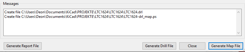
6. Click Generate Map File. 7. The result is shown in the Messages box of the Generate Drill Files window shown in figure 1.15D below:
Fig. 1.15D: Results in Messages box of the Generate Drill Files
8. In the Messages box it is shown that the following files are created: 9. -drl_map.ps.
10. These files must be given to a manufacturer to manufacture your PCB.
11. Click Close to close the Generate Drill Files window.
12. Click Close again to close the Plot window.
View the Gerber Files
Front Layer
1. In KiCad (5.1.2) click on Gerber Viewer (icon with black PCB and GBR written
on the lower right.
2. The Gerbview window opens.
3. Click File and click Open Excellon Drill File(s) … .
4. Select file with .drl extension.
5. This shows the component's legs holes and via holes as in figure 1.15E below:
Fig. 1.15E: Drill Files Showing Holes of Component's Legs and Via Holes
6. Click File and click Open Gerber File(s) …
7. Select the file with – Edge_Cuts.gm1 file extension.
8. You should see the outline of the board as shown in figure 1.15F below:
Fig. 1.15F: Edge_Cuts File Showing Outline of Board
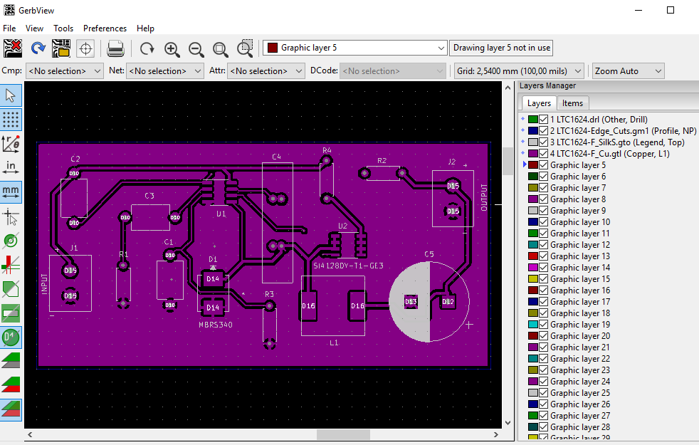
9. Click File and click Open Gerber File(s) … .
10. Select the front silkscreen file or the file with the -F.SilkS.gto file extension.
11. The front silkscreen file can be seen in figure 1.15G below:
Fig. 1.15G: Front Silk Screen
12. From the above, you can see the holes and vias line up with the silkscreen.
13. Click File and click Open Gerber File(s) … .
14. Select the front copper file or the file with the -F_Cu.gtl file extension.
15. The front copper file is now added to the previous files as shown in figure 1.15H
below:
Fig. 1.15H: Front Copper File Showing the Front Copper Track or Layer
16. Click File and click Open Gerber File(s) … .
17. Select the front solder mask file or the file with the -F_Mask.gts file extension.
18. Turn off the front copper layer file by unselecting the checkbox.
19. Otherwise, you won't see the front solder mask file.
20. The front solder mask file is now also added to the previous files and can be seen
in figure 1.15I below comprising brown-red circles and squares:
Fig. 1.15I Front Solder Mask Shown With Front Copper Turned Off
22. Remember the files with the F.Mask and B.Mask extensions define the area
that is free of solder mask.
23. It is the negative of the resulting solder mask film that covers the board.
24. The brown-red circles and squares show where the solder will be deposited
in order to connect the components.
25. As you open the layer files, they are allocated to a Graphic layer by a number
which is indicated by the Layers Manager window on the right.
26. In the Layers Manager, you can select a layer by clicking on the blue diamond on
the left.
27. You can also by selecting the checkbox of a layer display the layer or by
deselecting not display a particular layer.
28. When finished close Gerbview.
Repeat For the Back Layers
1. Repeat the process for the back layers.
2. Once again click File and click Open Excellon Drill File(s) … .
3. Select file with .drl extension.
4. Also, select the file with – Edge_Cuts.gm1 file extension so you can see the outline
of the board.
5. This shows the component's legs holes and via holes as in figure 1.15E above:
6. Click File and click Open Gerber File(s) … .
7. Open the back-solder mask file or the file with the -B_Mask.gbs file extension.
8. The back-solder mask file is where the back-solder mask file -B_Mask.gbs file should
line up with the drill hole layer as shown in figure 1.15J below:
Fig. 1.15J: Back Solder Mask Layer Lines Up With Drill Hole File
9. Also, load the back copper and back silkscreen files.
10. In figure 1.15K below is shown the drill hole layer. solder mask layer and back
copper layer.
Fig. 1.15K: Drill Layer Back Solder Mask and Copper Layer
11. Check that everything lines up.
12. As you open the files, they are allocated to a Graphic layer by a number which
is indicated by the Layers Manager window on the right.
13. In the Layers Manager, you can select a layer by clicking on the blue diamond
on the left.
14. You can also by selecting the checkbox of a layer display the layer or by deselecting
not display a particular layer.
15. By turning the layers on and off you can check if everything lines up.
1. Select a footprint. 2. Right-click and select Move. 3. Move the footprints apart.
4. The white lines are called air wires.
5. They are collectively known as a rat’s nest.
6. Move and rotate footprints until you have the least number of air wire crossings.
7. I follow the circuit drawing in my placing of footprints. 8. After placement of the footprints, it should be as in figure 1.14A below:
Fig. 1,14A: After Placement of The Footprints
Draw Board Edge or Outline of Printed Circuit Board (PCB)
1. Select Edge.Cuts layer on the right in the Layers Manager under Layers. 2. Click on the Place menu and select Line.
3. You can also on the right click on the icon with blue lines connected by green dots 4. Draw a box around the components to form the outline PCB.
Draw Left Vertical Line
1. Select the left vertical line and right-click. 2. Select Properties … E. 3. Line Properties window opens. 4. Set 4.1. Start point X: 4,1 in 4.2. Start point Y: 5,3 in 4.3. End point X: 4,1 in 4.4. End point Y: 3,2 in 4.5. Item thickness: 5,0 mils 4.6. Layer: Edge.Cuts 4.7. Click OK.
Draw Top Horizontal Line
1. Select the left vertical line and right-click. 2. Select Properties … E. 3. Line Properties window opens. 4. Set 4.1. Start point X: 4,1 in 4.2. Start point Y: 3,2 in 4.3. End point X: 7,7 in 4.4. End point Y: 3,2 in 4.5. Item thickness: 5,0 mils 4.6. Layer: Edge.Cuts 4.7. Click OK.
Draw Right Vertical Line
1. Select the left vertical line and right-click. 2. Select Properties … E. 3. Line Properties window opens. 4. Set 4.1. Start point X: 7,7 in 4.2. Start point Y: 5,3 in 4.3. End point X: 7,7 in 4.4. End point Y: 3,2 in 4.5. Item thickness: 5,0 mils 4.6. Layer: Edge.Cuts 4.7. Click OK.
Draw Bottom Horizontal Line
1. Select the left vertical line and right-click. 2. Select Properties … E. 3. Line Properties window opens. 4. Set 4.1. Start point X: 4,1 in 4.2. Start point Y: 5,3 in 4.3. End point X: 7,7 in 4.4. End point Y: 5,3 in 4.5. Item thickness: 5,0 mils 4.6. Layer: Edge.Cuts 4.7. Click OK.
Move Footprints onto the Board
1. Move the footprints onto the board. 2. The circuit with the current in each track is shown in figure 1.14B below:
Fig, 1.14B: Circuit with Current In Each Track
3. Once again spread the footprints that you have a minimum of crossings on the board.
Route The Tracks
1. It should be kept in mind when routing the tracks the pads of the surface-mounted
components are on the front copper layer.
2. These pads are therefore only directly accessible on the front copper layer.
3. It is the layer indicated by a maroon, brown-reddish color, and abbreviated F. Cu.
4. The through-hole components are accessible on both the front and back copper layer.
5. The back copper layer is indicated with a green color and abbreviated as B. Cu.
For Maximum of 2A Tracks
1. For a maximum of 2A in Pcbnew select from the above dropdown list:
Track: 22,00 mils (0,559 mm) and Via: 36,0/18 mils (0,91/0,46mm) 2. Click on Route tracks icon. 3. It is the icon on the right with the green squiggly line. 4. Then do the power tracks mostly on the Front Copper (F.Cu) layer.
For Maximum of 100mA Tracks
1. Now do the low current (below 100mA) signal tracks. 2. In Pcbnew select from the above dropdown list: Track: 10,00 mils (0,254 mm) and Via: 20,0/10,0 mils (0,51/0,25mm) 3. Click on Route tracks icon. 4. It is the icon on the right with the green squiggly line from the top left corner to the right bottom corner. 5. Then do the signal tracks on the Back Copper (B.Cu) layer. 6. Do not do the ground connections at this stage. 7. Use vias to jump over tracks if you have to. 8. The circuit with the routed tracks is shown in figure 1.14C below:
Fig. 1.14C: Circuit With Routed or Traced Tracks 9. The white lines or air wires are the ground connections which will be connected with a copper fill.
Copper Fill
Front Copper Layer
1. Select the Front Copper (F.Cu) layer. 2. Select the Filled zones tool on the right. 3. It is the icon with a square green background and a grey annular pad and track. 4. Click on the viewing area. 5. The Copper Zone Properties window opens as shown in figure 1.14D below.
Fig. 1.14D: Copper Zone Properties
6. Under Net select GND. 7. Click OK. 8. Draw the fill rectangle close around the outer edge of the board 9. Double click to end selection.
10. The filled Front Copper (F.Cu) layer should look as in figure 1.14E below.
Fig. 1.14E: Filled Front Copper Layer
Back Copper Layer
10. Now do the same for the Back Copper (B.Cu) layer. 11. Also select ground GND. 12. This project does not have a VCC Net. 13. In the end, the filled back copper layer should look something like in figure 1.14F below.
Fig. 1.14F: Filled Back Copper Layer
Place Version Number
1. Select Add ext to copper layers or graphic text the T icon and B.SilkS layer. 2. Type “V-01”. 3. The copper fill on the back copper layer and the version number is shown in figure 1.14G below:
Fig. 1.14G: Version Numer V-01 on Back Silk Screen
4. A close-up of the copper fill on the back copper layer and the version number is shown in figure 1.14H below:
Fig. 1.14H: Close-Up of Version Number V-01 on Back Silk Screen