Part A: Annotate and Edit Component Symbols
1. Open the schematic of your circuit or Eeschema.
2. At the moment the symbols have labels like R?, C?, U? and RV?.
3. The "?" indicates a number has not been allocated.
4. You can add these by hand if you want to give them specific numbers.
2. At the moment the symbols have labels like R?, C?, U? and RV?.
3. The "?" indicates a number has not been allocated.
4. You can add these by hand if you want to give them specific numbers.
5. This, however, can be done automatically with KiCad.
6. In Eeschema click Tools and then click Annotate Schematic … .
7. The icon is a page with a pencil from the bottom left towards the upper right of the
page.
8. The Annotate Schematic window appears.
9. Click Annotate
10. Messages appear in the Annotation Messages: window
11. Click Close.
12. You will notice that all the symbols are now numbered.
Edit the Si4128DY Symbol
1. Right-click Si4128DY.
2. Click Properties and click Edit with Library Editor.
2. Click Properties and click Edit with Library Editor.
3. The Symbol Editor window opens.
4. Right-click on pin 1 and click on Edit … .
5. The Pin Properties window opens.
6. Set:
6.1. Pin name: Source.
6.2. Electrical type: Output.
6.3. Click OK.
Pin 2 and 3
1. Right Click on pin 2 and click on Edit … .
2. The Pin Properties window opens.
3. Set:
3.1. Pin name: Source.
3.2. Electrical type: Output.
3.3. Click OK.
4. Do the same for pin 3.
Pin 4
1. Right Click on pin 4 and click on Edit … .
2. The Pin Properties window opens.
3. Set:
3.1. Pin name: Gate.
3.2. Electrical type: Input.
3.3. Click OK
Pins 5, 6, 7 and 8
2. The Pin Properties window opens.
3. Set:
3.1. Pin name: Drain.
3.2. Electrical type: Input.
3.3. Click OK
4. Do the same for pins 6, 7 and 8.
5. The symbol should eventually look as in figure 1.3A below:
 |
| Fig. 1.3A: Edited MOSFET Transistor with 3 Source Output Pins. |
Part B: Electrical Rules Checker
2. It is the icon with a bug.
3. The Electrical Rules Checker window opens as shown in figure 1.3B below.
 |
| Fig. 1.3B: Electrical Rules Checker |
4. Click Run.
5. We have 5 warnings as shown in figure 1.3C below:
7. From the first two in the errors list given by KiCad above, KiCad is
unhappy that pins 1, 2 and 3 which are all outputs of U2 or MOSFET
transistor si4128 are connected together.
8. The reason for this is when we click on the Options tab and we see the following
in figure 1.3D below:
9. From the second row from the top, we see that if an output pin is
connected to an output pin an error message is generated.
10. We have a bit of a unique situation here.
11. The reason mainly why there are multiple pins used is to conduct
the heat generated in the MOSFET transistor.
.
12. You can read more here.
13. Personally, I think it is also to lower the electrical resistance.
14. I could, however, find nothing to support my thinking.
15. Further, I do not like to have outputs not connected to something.
16. We have to fool KiCad to accept the connection of the source output pins
connected together.
17. As can be seen in the above figure in the case of a passive pin, no matter if it is
connected to input, output - , bidirectional - , tri-state-, or passive pin, it would
not generate an error.
18. So if we change pins 2 and 3 to passive pins they would not generate any errors.
1. Right-click Si4128DY.
2. Click Properties and click Edit with Library Editor.
3. The Symbol Editor window opens.
4. Right Click on pin 2 and click on Edit … .
5. The Pin Properties window opens.
6. Set:
6.1. Pin name: Leave as Source.
6.2. Electrical type: Chane to Passive.
6.3. Click OK.
7. Do the same for pin 3.
8. The symbol for si4128dy should now look like as shown in figure 1.3E below:
9. Now run the Electrical Rules Checker again.
10. You should see the following as shown in figure 1.3F below:
11. All the errors are gone.
12. For now, we can ignore the warnings.
13. Click Close.
Previous: Tutorial 1.2 Import Symbol Continue With Drawing of Circuit
Next: Tutorial 1.4: Assign Footprints
 |
| Fig. 1.3C: Results Electrical Rules Checker 2 Errors 2 Warnings |
7. From the first two in the errors list given by KiCad above, KiCad is
unhappy that pins 1, 2 and 3 which are all outputs of U2 or MOSFET
transistor si4128 are connected together.
8. The reason for this is when we click on the Options tab and we see the following
in figure 1.3D below:
 |
| Fig, 1,3D: Error and Warning Tables Under Options Tab |
connected to an output pin an error message is generated.
10. We have a bit of a unique situation here.
11. The reason mainly why there are multiple pins used is to conduct
the heat generated in the MOSFET transistor.
.
12. You can read more here.
13. Personally, I think it is also to lower the electrical resistance.
14. I could, however, find nothing to support my thinking.
15. Further, I do not like to have outputs not connected to something.
16. We have to fool KiCad to accept the connection of the source output pins
connected together.
17. As can be seen in the above figure in the case of a passive pin, no matter if it is
connected to input, output - , bidirectional - , tri-state-, or passive pin, it would
not generate an error.
18. So if we change pins 2 and 3 to passive pins they would not generate any errors.
Edit Si412DY Symbol Again
2. Click Properties and click Edit with Library Editor.
3. The Symbol Editor window opens.
4. Right Click on pin 2 and click on Edit … .
5. The Pin Properties window opens.
6. Set:
6.1. Pin name: Leave as Source.
6.2. Electrical type: Chane to Passive.
6.3. Click OK.
7. Do the same for pin 3.
8. The symbol for si4128dy should now look like as shown in figure 1.3E below:
 |
| Fig. 1.3E: Edited Si4128dy MOSFET with 2 Passive Source Pins. |
9. Now run the Electrical Rules Checker again.
10. You should see the following as shown in figure 1.3F below:
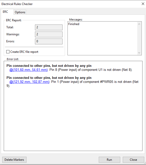 |
| Fig. 1.3F: All the Errors are Gone |
11. All the errors are gone.
12. For now, we can ignore the warnings.
13. Click Close.
Previous: Tutorial 1.2 Import Symbol Continue With Drawing of Circuit
Next: Tutorial 1.4: Assign Footprints
No comments:
Post a Comment