The Circuits
 |
| Fig. 1.9A: Eeschema Circuit |
2. The LTspice XVll simulation circuit of the Eeschema circuit is shown in figure 1.9B
below:
 |
| Fig. 1.9B: LTspice Simulation Circuit. |
Calculate The Power Consumption In The Resistors
Watch this video on Youtube Calculate Power in Resistors Using LTspice
Power Consumption in Resistor (10 R1 - 6.8k) in Eeschema
1. The power plot or light blue trace of R1 - 6.8kohm in Eeschema (R3 in
LTspice circuit) is shown in figure 1.9C below:
 |
| Fig. 1.9C: Power Graph in R1 |
2. The power in R1 in Eeschema starts at 0 then goes up to 23uW after 0.05ms.
3. The power thereafter remains at zero and then at 0.25ms goes briefly to 6uW.
4. The average power in R1 as calculated by LTspce in R1 over a period of 1ms is
403.59nW.
5. The point is the power consumption in R1- 6.8kohm in Eeschema
(R3 in LTspice circuit) is very low so a normal 250mW resistor should be more
than adequate.
Power Consumption in (11 R2 - 35.7k) in Eeschema
LTspice circuit) is shown in figure 1.9D below:
 |
| Fig. 1.9D: Power Graph in R2 |
2. From the light blue trace, it can be seen that the power consumption in R2 starts at 0.
3. After 0.1ms it starts to rise until at about 0.25ms it reaches about 130uW.
4. After a slight overshoot, it settles at 130uW.
5. The average power in R2 as calculated by LTspce in R2 over a period of 1ms is
104.37uW.
5. A normal 250mW resistor should be more than adequate.
Power Consumption in R3 - 20K ohm in Eeschema
LTspice circuit) is shown in figure 1.9E below:
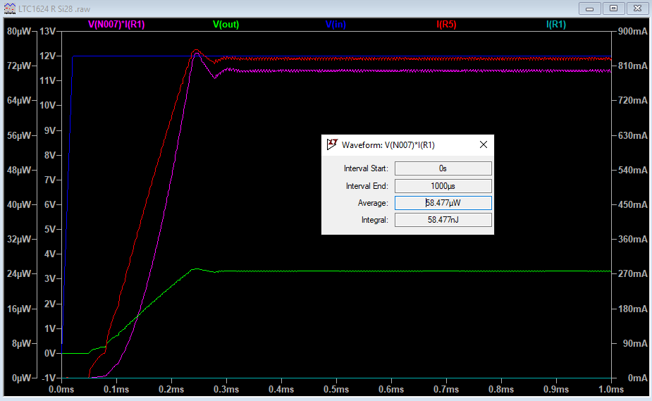 |
| Fig. 1.9E: Power Graph in R3 |
2. From the purple trace or plot, it can be seen that the power consumption in
R3 starts at 0.
3. After 0.1ms it starts to rise until at about 0.25 ms it reaches about 73 uW.
4. After a slight overshoot, it settles at roundabout 71uW.
5. The average power in R3 as calculated by LTspce in R3 over a period of 1ms is
58.477uW.
6. A normal standard 250mW resistor should be more than adequate.
Power Consumption in R4 - 0.033 ohm in Eeschema
LTspice circuit) is shown in figure 1.9E below:
 |
| Fig. 1.9E Power Trace Plot in Resistor R4 0.033 Ohm |
2. From the red trace or plot, it can be seen that the power consumption in R4
starts at approximately 0.08ms at a peak of 0.9W
3. After 0.1ms it starts to rise until at about 0.15 ms it reaches a peak of about 1.4W.
4. It then drops down to a peak of about 1.3W after 0.25ms.
5. After that, it collapses completely to 0W at 0.28ms.
6. It then wakes up at 0.29 ms raises briefly to perhaps a peak of 0.3W.
7. After about 0.35ms it never exceeds a peak of 0.2W.
8. We can thus say after 0.28ms or 280us a normal standard 250 mW resistor should
be more than adequate.
9. The question is what about the time period between 0.1 ms (100us) and
0.28ms 280us?
10. We can ask LTspice to expand the graph and then we get the power consumption in
R4 in the period of 0.1 ms (100us) and 0.28ms (280us) shown in figure 1.9F below.
 |
| Fig. 1.9F: Power Consumption in R4 during 60us - 280 us. |
11. We can ask LTspice to calculate the average power consumption which shown
in the square in the upper left and is estimated at 95.38mW.
12. Once again a normal standard 250 mW resistor should be able to handle this.
Current in R4 0.033 Ohm Resistor
1. We may as well look at the current in R4 the 0.033 Ohm resistor.
2. The Current plot in the R4 resistor is shown in figure 1.9G below:
 |
| Fig. 1.9G: Current in R4 0.33 Ohm Resistor |
3. We can say that the current in R4 peaks at 6.6A in the first 0.25 ms and after about 0.2
ms peaks at 2.4A.
4. Current in R4 in the time period between 80uS and 280uS is shown in figure 1.9H
below:
 |
| Fig. 1.9H: Current in R4 between 100uS and 280uS. |
5. Over the time period of (80-280)us we can say the average current is 736.35mA and
root mean square value is 1.7822A.
6. Current in R4 after 0.21 ms is shown in figure 1.9I below:
 |
| Fig. 1.9I: Current in R4 after 0.28ms |
7. The current for the time period between 210us to 1ms is on average 281.04mA and
the RMS value is 671.75mA.
KiCad Resistor Footprint Format
1. Footprints are grouped into libraries (directories with .pretty extension) based on
their primary function.
2. Each footprint is a .kicad_mod file (stored within a .pretty directory).
Axial Resistors
1. The format for axial resistors is:
R_Axial_L[Length]_D[Diameter]_P[Pitch]_[Modifiers]_[Orientation]_[Options]
2. Where:
2.1. L - Length - Resistor body length.
2.2. D - Diameter - Body diameter.
2.3. P - Pitch - Lead spacing.
2.4. Modifiers - Modifiers to footprint specifications (Optional).
2.5. Orientation - Resistor orientation (Vertical / Horizontal) (Optional).
2.6. Options - Extra footprint options (Optional).
4. This means the leads of the resistor are axial, the body length of the resistor is
3.6 mm, the diameter of the resistor is 1.6 mm, the spacing between the leads are
5,08 mm and the footprint is for a horizontally mounted resistor.
Choose Resistor Footprint and Assign Resistor Footprint to Resistors
You can watch this video on YouTube by clicking on choose and assign resistor footprint.
Choose Resistors for R1, R2 and R3
1. A good choice for resistors would be the Vishay MBA/SMA 0204 series.
2. The datasheet can be found at Vishay
3. Particulars of the resistors appear in figure 1.9J below:
 |
| Fig. 1.9J: Particulars of Vishay Resistors |
4. The technical specifications are shown in figure 1.9K below:
 |
| Fig. 1.9L: Technical Specification of Resistors |
5. From the above, we see that MBA/SMA 0204 has a DIN size of 0204, resistance range
0,22 Ohm to 10 Mega Ohm and a rated dissipation of 0.4 W.
6. The resistor dimensions are shown in figure 1.9L below:
7. The MBA/SMA 0204 resistors have:
7.1 L = 3.0 mm.
7.2 D = 1.6 mm.
7.3 M (or P in KiCad) = 5.0 mm.
6. The resistor dimensions are shown in figure 1.9L below:
 |
| Fig. 1.9L: Resistor Dimensions |
7.1 L = 3.0 mm.
7.2 D = 1.6 mm.
7.3 M (or P in KiCad) = 5.0 mm.
8. Re-written in KiCad format it would be: R_Axial_L3.6mm_D1.6mm_P5.00mm.
Assign Footprints to Resistors R1, R2 and R3
Assignments click on 10 R1 - 6.8k :.
2. In the left column under Footprint Libraries click on Resistor_THT.
3. In the right column under Filtered Footprints double click on
Resistor_THT:R_Axial_DIN0204_L3.6mm_D1.6mm_P5.08_Horizontal
4. Click on View selected footprint icon.
5. It is the icon with the vertical IC with red legs and magnifying glass in the lower
right corner.
6. The footprint should be as shown in figure 1.9M below:
 |
| Fig. 1.9M: Resistor Footprint |
7. Click on the 3D Display icon.
8. It is the icon with a square dark grey component mounted in a green PCB board
viewed from the side.
9. It is shown in figure 1.9N below:
 |
| Fig. 1.9N: 3D View of Resistor |
10. Click on Apply, Save Schematic & Continue.
11. Repeat for all the other resistors up and until 12 R3 - 20k:.
12. After all the resistors have been assigned footprints it should like in the
Assign Footprints window as shown figure 1.9O below:
 |
| Fig. 1.9O: Footprint Assignments to R1, R2 and R3 |
13. Click Apply, Save Schematic & Continue.
14. Click OK.
Choose Resistor and Design Resistor and Assign Footprint
You can watch this video on YouTube by clicking on design resistor footprint and
assign resistor footprint.
Choose Resistor for Symbol 13 Resistor R4 0.033 Ohm
2. Particulars of the resistors appear in figure 1.9P below:
 |
| Fig. 1.9P: 0,033 Ohm Resistor on element 14 website |
3. It costs $2.15 for one.
4. For the technical datasheet of the resistor click on SBL4R033J
5. The particulars of Tyco Electronic low ohmic current sense resistors are shown in
figure 1.9Q.
 |
| Fig. 1.9Q: Low Ohmic Current Sense Resistors |
6. The dimensions for the low ohmic resistors are shown in figure 1.9R below:
 |
| Fig. 1.9Q Dimensions of Low Ohmic Current Sense Resistors |
Design Footprint For Resistor R4 0.033 Ohm
1. Open the Footprint Editor.
2. Click File and select New Footprint ...
3. Type in the name:
THT_R_Axial_L18mm_D6.4mm_P40.00_Horizontal.
4. Click OK.
5. Click File and select Save.
6. Choose in my case the KICADFootprints library.
Draw Pad1
2. Set the pad properties as in figure 1.9R below:
 |
| Fig. 1.9R: Properties of Pad1 of Resistor Footprint |
3. Click OK.
Draw Pad2
2. Set the pad properties as in figure 1.9R below:
 |
| Fig. 1.9R: Properties of Pad 2 of Resistor |
3. Click OK.
Draw The Front Fabrication Layer of The Footprint
components on the PCB. The recommended line width is 0.1mm.
Draw The Top Horizontal Line of Mechanical Outline
2. Draw a horizontal line.
3. Set the properties of the line as in figure 1.9S below:
 |
| Fig. 1.9S: Fabrication Layer Top Horizontal Line |
4. Click OK.
Draw The Bottom Horizontal Line of Mechanical Outline
2. Draw a horizontal line opposite and below the top horizontal line.
3. Set the properties of the line as in figure 1.9T below:
 |
| Fig. 1.9T: Fabrication Layer Bottom Horizontal Line |
4. Click OK.
Draw The Left Vertical Line of Mechanical Outline
2. Draw a vertical line to the left and between the top and bottom horizontal lines.
3. Set the properties of the line as in figure 1.9U below:
 |
| Fig. 1.9U: Fabrication Layer Left Vertical Line |
Draw The Right Vertical Line of Mechanical Outline
2. Draw a vertical line to the left and between the pad and bottom horizontal lines.
3. Set the properties of the line as in figure 1.9V below:
 |
| Fig. 1.9V: Fabrication Layer Right Vertical Line |
4. Click OK.
Draw Left Horizontal Line Pad To Body (Left Terminal Outline)
2. Draw a vertical line to the left and between pad 1 and body vertical line.
3. Set the properties of the line as in figure 1.9W below:
 |
| Fig. 1.9W: Fabrication Layer Left Terminal Outline |
4. Click OK.
Draw Right Horizontal Line Pad To Body (Right Terminal Outline)
2. Draw a horizontal line to the right and between pad 2 and body vertical line.
3. Set the properties of the line as in figure 1.9X below:
 |
| Fig. 1.9X: Fabrication Layer Right Terminal Outline |
4. Click OK.
REF** Text On Fabrication Layer
1. In the Footprint Editor click Add Text.
2. Type " %R" in the Text box of the Footprint Text Properties window.
3. In the Layer drop-down list choose F.Fab.
4. The Footprint Text Properties should be as in figure 1.9Y below:
 |
| Fig. 1.9Y: Footprint Text Properties of REF** |
Silkscreen Layer
1. The silkscreen is printed to the external surface of a PCB to aid in
the component identification and orientation.
2. This layer contains the component RefDes (reference designator) to
locate components on the board after assembly.
3. Silkscreen line width should nominally be 0.12 mm.
Draw Horizontal Lines
1. In the Footprint Editor click Add graphic line.
2. Draw the top horizontal line just above the top horizontal line in the fabrication layer.
3. Set the properties of the line as in figure 1.9Z below:
 |
| Fig. 1.9Z: Silkscreen Layer Top Horizontal Line |
4. Click OK.
5. Draw the bottom horizontal line in the same manner except set Start point Y:
and End point Y: at 3,3.
1. In the Footprint Editor click Add graphic line.
2. Draw the left vertical line between the horizontal lines on the left.
3. Set the properties of the line as in figure 1.9AA below:
Draw Vertical Lines
1. In the Footprint Editor click Add graphic line.
2. Draw the left vertical line between the horizontal lines on the left.
3. Set the properties of the line as in figure 1.9AA below:
 |
| Fig. 1.9AA: Left Vertical Line in Silkscreen Layer |
4. Click OK.
5. Draw the right vertical line on the right, between the horizontal lines.
6. The only difference is that Start point X: and End point X: is at 9,1.
Draw The Horizontal Lines Pad To Body
2. Draw the left horizontal line to the right and between pad 2 and the vertical line
of the body.
3. Set the properties of the line as in figure 1.9BB below:
 |
| Fig. 1,9BB: Silkscreen Left Horizontal Line Pad To Body |
4. Click OK.
5. Draw the right horizontal line on the right, between the vertical body line and pad 2.
6. The only difference is that Start point X: is at 9,1 and End point X: is at 18,5.
REF** Text On Silkscreen Layer
1. In the Footprint Editor click Add Text.
2. Type " REF**" in the Text box of the Footprint Text Properties window.
3. In the Layer drop-down list choose F.SilkS.
4. The Footprint Text Properties should be as in figure 1.9CC below:
5. Click OK.4. The Footprint Text Properties should be as in figure 1.9CC below:
 |
| Fig. 1.9CC: Silkscreen Layer REF** |
Courtyard Layer
1. The component courtyard is defined as the smallest rectangular area that
provides a minimum electrical and mechanical clearance around the combined
component body and land pattern boundaries.
2. It is allowed to create a contoured courtyard area using a polygon instead of a
simple rectangle. (IPC-7351C).
3. Courtyard uses line width 0.05mm.
4. All courtyard line elements are placed on grid of 0.01mm.
5. Unless otherwise specified, clearance is 0.25mm.
6. Connectors, Canned capacitors and crystals should have a clearance of 0.5mm.
7. BGA devices should have a clearance of 1.0mm.
8. Kicad example of courtyard layer is shown in figure 1.9CCA below:
 |
| Fig. 1.9CCA: Kicad example of courtyard layer |
9. See Kicad Courtyard Layer Requirements.
Draw Horizontal Lines of Courtyard Layer
2. Draw the top horizontal line just above the top horizontal line in the fabrication layer.
3. As far as the total width of the courtyard is concerned, take: the pitch width along an
axis + the radius of the pad.
4. This gives us 20mm + 2.5mm/2 = 21.25mm.
5. To this, we must add 0.25mm courtyard clearance = 21.25mm + 0.25mm = 21.50mm.
6. However, let's make it 22mm.
7. As far as the height is concerned we already have the top horizontal silkscreen
line at 3.3mm.
8. If we add 0.25mm for courtyard clearance then we have 3.3mm + 0.25mm
= 3.55mm.
9. So let us make that then at 3.6mm.
10. Set the properties of the line as in figure 1.9DD below:
 |
| Fig. 1.9DD: Horizontal Line of Courtyard |
11. Click OK.
5. Now draw the bottom horizontal line on the courtyard layer.
5. The only difference set Start point Y: and End point Y: at 3,5mm.
Draw Vertical Lines of Courtyard Layer
1. In the Footprint Editor click Add graphic line.
2. Draw the left vertical line between the horizontal lines on the left.
3. Set the properties of the line as in figure 1.9EE below:
 |
| Fig. 1.9EE: Vertical Line of Courtyard |
4. Click OK.
5. Draw the right vertical line between the horizontal lines on the right.
6. The only difference set Start point X: and End point X: to 22.
7. Finally, the footprint for symbol 13, resistor R4 of 0.033 Ohm is as shown in
figure 1.9FF:
 |
| Fig. 1.9FF: Footprint for 0.033 Ohm Resistor |
8. Assign footprint to 13. R4 0,033 ohm as is shown in figure 1.9GG below:
 |
| Fig. 1.9GG: Footprint Assigned To 13 R4 0.033 Ohm Resistor |
Let me know if you notice any mistakes.
No comments:
Post a Comment