Assign Footprint to (6 D1- MBRS340)
1. KiCad has already assigned to D1- MBRS340 footprint:
Diode_THT:D_DO-201AD_P15.24mm_Horizontal.
2. If we click on View selected footprint, we see the following as shown in
figure 1.6A below:
 |
| Fig. 1.6A: Diode Footprint |
3. Click on 3D Display (Alt+3).
4. We see the 3 D view of the diode in figure 1.6B below:
 |
| Fig. 1.6B: 3 D View of Diode |
5. This is for the through-hole technology diode.
6. If we want a surface mount diode footprint, we will have to create one.
Footprint Library tables
tool based on footprint library tables which allows direct use of footprint libraries
from:
1.1. KiCad Legacy footprint libraries (.mod files).
1.2. KiCad New, .pretty footprint libraries (on your local disk) (folders with
.pretty extension, containing .kicad_mod files).
1.3. KiCad New, .pretty footprint libraries (on the KiCad Github server,
or other Github server).
1.4. GEDA libraries (folders containing .fp files).
1.5. Eagle footprint libraries.
2. The nickname is used to look up footprints instead of the previous method which
depended on library search path ordering.
KiCad Library Convention
Footprint Libraries
1. Footprints are grouped into libraries (directories with .pretty extension) based on
their primary function.
2. As an extension of this, footprint libraries should be named based on this same
functionality.
3. Library names must be defined based on the priority list below, with each
element separated by the underscore (_) character:
3.1. Function (e.g. Conn, Capacitor).
3.2. Sub-function (e.g. HDMI, USB).
3.3. Tertiary qualifier (e.g. RightAngle, SMD).
3.4. Manufacturer name (e.g. Texas, Microchip).
3.5. Footprint series name (e.g. MicroFit).
3.6. Extra library descriptors as required.
4. Some of the elements listed above may be omitted if not required.
5. Examples footprint library names:
5.1. Conn_USB_SMD - Surface mount USB connectors.
5.2. Conn_Molex_MicroFit - Molex MicroFit series rectangular connectors.
5.3. Capacitor_Tantalum_SMD - Surface mount Tantalum capacitors.
Download, Edit and Assign a Diode Footprint
Download Diode Footprint Ultra Librarian
1. KiCad does not have an MBRS340 diode footprint,
you can, however, try and download it from Ultra Librarian.
2. You will find the footprint for the ON Semiconductor MBRS340T3G Schottky
Power Rectifier, Surface Mount 3.0 A 40 V MBRS340 diode footprint.
3. There is no exact match for MBRS340.
4. Ultra Librarian proposes the following as seen in figure 1.6C below:
 |
| Fig, 1,6C: Footprints Proposed by Ultra Librarian for Diode MBRS340 |
5. Choose and download MBRS340T3G.
6. Save the footprint on your computer.
7. I saved it as footprint MBRS340 under Kicad footprint library Diodes.pretty file as can
be seen in figure 1.6D below:
 |
| Fig. 1,6D: Footprint MBRS340.kicad_mod Saved Under Kicad Library Diodes.pretty File |
Add Diode Library
1. In the Assign Footprints window click on Preferences and
Manage Footprint Libraries … .
2. The Footprint Libraries window opens as shown in figure 1.6E below:
 |
| Fig. 1.6E: Footprint Libraries Window |
3. Scroll to the end of the list.
4. Click on the Add existing library to table.
5. It is the File icon.
6. Navigate to where you stored the Ultra Librarian file MBRS340 footprint file on your
computer.
7. It has a .pretty extension.
8. Select it.
9. Give it the Nickname "MBRS340" so you can recognize it.
10. Click OK.
11. Give KiCad some time to settle down.
Investigate the Diode Footprint MBRS340
1. With the MBRS340 footprint selected click on View selected footprint.
2. It is the icon with the vertical IC with red legs and magnifying glass in the lower right.
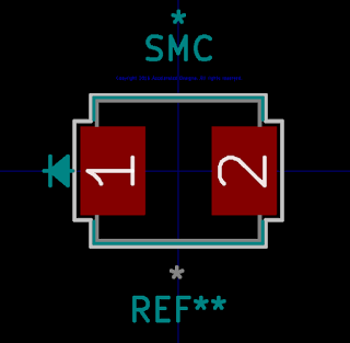
3. It should look like shown in figure 1.6F below:
 |
| Fig. 1.6F: Diode MBRS340TG Footprint |
4. One cannot make out the text in the middle.
5. Open it in the Footprint Editor.
6. Select "*", "REF**" and "SMC" and move it up and above out of the footprint itself.
7. Click Save.
8. It should now look like in figure 1.6F below:
 |
| Fig. 1.6G: Diode Footprint With Text Moved |
9. Click Save.
The Dimensions of Diode Footprint MBRS340
1. The Fairchild now the ON Semiconductor datasheet suggests the following as
far as MBRS340T Schottky Power Rectifier in regard to its
footprint dimensions concerned as shown in figure 1.6H below:
 |
| Fig. 1.6H: Footprint Dimensions of Diode MBRS340 |
2. We can use the KiCad Vernier Calliper tool to measure the dimensions of the
pads and the distance between the pads of the footprint, we have chosen for the
diode.
3. The following table, table 1 below was compiled indicating the differences between
the measured dimensions and recommended dimensions for the MBRS340 diode:
 |
| Tabel1: Differences Between Measurements of Footprint and Data Sheet of Footprint |
4. It seems thus that the pads are a bit bigger than as recommended by
Fairchild ON Semiconductor.
5. Further, the pads seem to be too close
Edit Diode Footprint
so that it complies with the dimensions in the Fairchild datasheet.
2. In Eeschema click on the horizontal IC icon to open the Footprint Editor.
3. In my case under Diodes (Diodes.pretty) double-click on MBRS340
(MBRS340.kicad_mod).
.
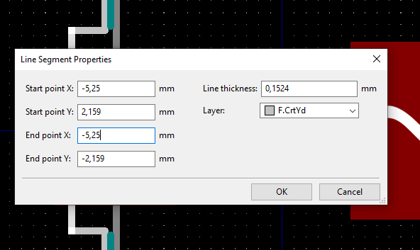
Edit Left Vertical Line of Footprint
2. Right-click select Properties and set:
2.1. Start point X: -5,25 mm and
2.2. End point Y: -5,25 mm as in figure 1.6I below:
 |
| Fig. 1.6I: Left Vertical Line of Footprint |
Edit Pad 1
2. Right-click select Properties and set:
2.1. Position X: -3.6 mm which is half of 7.2 mm the distance between
the center of the pads.
2.2. Seize X: 2.6 mm according to the datasheet and
2.3. Seize Y: 3.2 mm according to the datasheet and as in figure 1.6J below:
 |
| Fig. 1.6J: Left Pad 1 of Footprint |
Edit Top Left Horizontal Line
2. Right-click select Properties....
3. Set Start point X: -5,25 mm as in figure 1.6K below:
.
 |
| Fig. 1.6K: Top Left Horizontal Line of Footprint |
Edit Bottom Left Horizontal Line
2. Right-click select Properties...
3. Set End point X: -5,25 mm as in figure 1.6L below:
 |
| Fig. 1.6L: Bottom Left Horizontal Line of Footprint |
Edit Right Vertical Line of Footprint
1. Select the right vertical line.
2. Right-click select Properties… and set:
2.1. Start point X: 5,25 mm and
2.2. Endpoint Y: 5,25 mm as in figure 1.6M below:
 |
| Fig. 1.6M: Right Vertical Line of Footprint |
Edit Pad 2 of Footprint
1. Select the right pad number 2.
2. Right-click select Properties… and set:
2.1. Position X: 3.6 mm, which is half of 7.2 mm the distance between the
center of the pads.
2.2. Seize X: 2.6 mm according to the datasheet and
2.3. Seize Y: 3.2 mm according to the datasheet and as in figure 1.6N below.
 |
| Fig. 1.6N: Pad 2 of Footprint |
Edit Top Right Horizontal Line
1. Select the top right horizontal line.
2. Right-click select Properties...
3. Set End point X: 5,25 mm as in figure 1.6O below:
 |
| Fig. 1.6O: Top Right Line of Footprint |
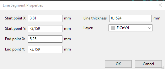
Edit Bottom Right Horizontal Line
1. Select the bottom right horizontal line.
2. Right-click select Properties…
3. Set Start point X: 5,25 mm as in figure 1.6P below:
 |
| Fig. 1.6P: Bottom Right Horizontal Line of Footprint |
4. Save footprint as MBRS340_Mod under Diodes.
5. The finished diode footprint is shown in figure 1.6Q.
5. The finished diode footprint is shown in figure 1.6Q.
 |
| Fig, 1,6Q: Finished Diode Footprint |
Assign Footprint to Diode (6 D1- MBRS340)
on nickname MBRS340_Mod that you allocated to the diode footprint.
2. In the middle Symbol: Footprint Assignments window make certain diode
6 D1- MBRS340: is selected.
3. Assign the footprint by double-clicking on Diodes: MBRS340_Mod on the right and
in the Filtered Footprints window.
4. It should look like as shown in figure 1.6Q below:
 |
| Fig. 1.6: Footprint Assigned to Diode MBRS340 |
5. Click Apply, Save Schematic & Continue.
Assign Footprints to (7 J1- ED2609-ND and 8 J1- ED2609-ND)
1. In Assign Footprints and in the Footprint Libraries and under
digikey-footprints assign
digikey-footprints:Term_Block_1x2_P5.08MM
by first selecting J1 and double-clicking on the footprint.
2. Do the same for J2.
3. The PCB layout of the terminal block is shown for a three-legged terminal as in
figure 1.6I below:
figure 1.6I below:
 |
| Fig. 1.6I: PCB Layout of the Terminal Block |
4. Click on View selected footprint.
5. The footprint as shown in figure 1.6J below appears:
 |
| Fig. 1.6J: Footprint for Terminal Block |
6. Use the Vernier caliper by clicking on the Measure distance between two points
icon.
7. The measured distances, when compared with datasheet values, are as follows:
7.1. The horizontal distance from the left side of the block to the center of
pin 1 is measured = 2.67 mm.
According to the datasheet, it should be 3.1 mm.
7.2. The diameter of the hole is measured = 0.76 mm.
According to the datasheet, it should be 1.3 mm.
7.3. The distance between pins are measured to be 5.08 mm.
According to the datasheet, it should be 5.08 mm.
7.4. The vertical distance from the center of the block to the lower side of
the block is measured at 4.06 mm.
According to the datasheet, it should be 4.2 mm.
8. This footprint does not seem to meet all the necessary requirements.
9. It would be better to create our own footprint for the connector of
DigiKey ED2609-ND.
10. We will do this next time.
Please let me know if I had made any mistakes.
Previous: Tutorial 1.5: Assign Capacitor Footprints and Create Capacitor Footprints
Next: Tutorial 1.7: Design Connector Footprint
No comments:
Post a Comment