Showing posts with label printed circuit board. Show all posts

Friday, 11 October 2019

Tutorial 1.11: Calculating the Currents in the PCB:


The Circuit in LTspice
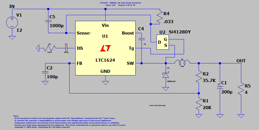

1.      The circuit in LTspice looks like shown in figure 1.11A below:


Fig. 1.11A: Circuit In LTspice


The Currents


1.    The drain current in U2 Si4128Dy is as shown in by the light blue trace 

       figure 1.11B below:


Fig. 1.11B: Drain Current in Si128DY Over 1ms.


2.     The drain current in Si4128DY in the time period of (60 – 280)us is shown in 

         figure 1.11C below.


Fig. 1.11C: Drain Current During Time Period of (60 - 280)us.


3.      The RMS value of the drain current during the period of (60-280)us = 1.7001A.

4.      The RMS value of the drain current in U2 over 1ms time period is 907.78mA as 

          shown in figure 1.11D below:


Fig. 1.11D: RMS Value of Drain Current of 1ms Time Period


5.      RMS Source current of U2 over a time period of 1ms = 907.66mA as shown in 

         figure 1.11E below:


Fig. 1.11E: Source Current U2 Over Time Period of 1ms


6.      The current in U1 LTC1624 pin SW up to 1ms = 63.165mA as shown in 

          figure 1.12F in the purple trace below:


Fig. 1.11F: Current in pin SW of U1 LTC1624 Over 1ms Time Period


7.      The current in inductor L1 is shown by the light blue trace in figure 1.11G below. 

8.      The RMS current in inductor l1 over a 1ms period = 1.9488A.
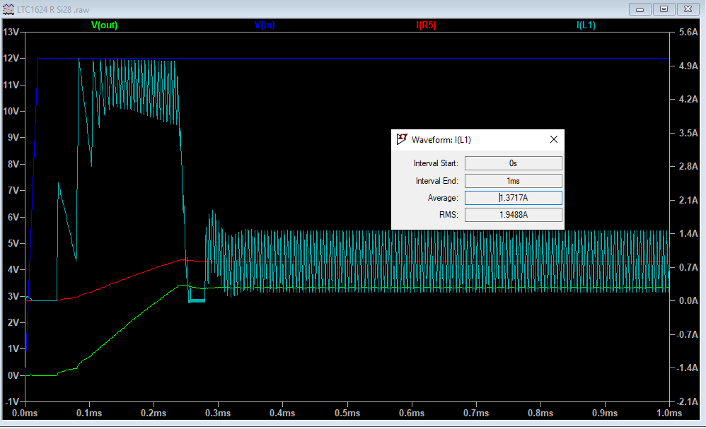


Fig. 1.11G: Current in Inductor L1 Over 1ms Period


9.     The current in the trace or wire between R2 and C1 as in the LTspice circuit in
        
         figure 1.11A above is shown in figure 1.11H below:


Fig. 1.11H: Current in Trace or Wire Between R2 and C1


10.    The current between R2 and C1 has an RMS value of = 1.9488A.

11.     From the above, we can conclude that the RMS value of the current does not 

          exceed 2A and reaches a peak value spikes of 6.4A over a period 

          of 280us - 60us = 220us.


Summary of Currents


A summary of current calculations from previous tutorials are shown in table 1.11A below:


Table 1.11A: Summary of Previous Current Calculations


A further summary of current calculations are shown in table 1.11B below:

Table 1.11B: Further Summary of Previous Current Calculations


KiCad Eeschema Circuit


The KiCad Eeschema circuit is shown for ease of reference in figure 1.11I below:


Fig. 1.11I: KiCad Eeschema Circuit


Input Current


1.     The input current in the conductor between IN pin V1 and capacitor C5 1000p in 
   

        the LTspice circuit is shown by the light blue trace in figure 1.11J below:


Fig. 1.11J: Conductor between IN pin V1 and capacitor C5 1000p Over Time Period of 1ms

2.     As can be seen from above the input current in the conductor between IN pin V1 

        and capacitor C5 1000p  over a time period of 1ms is 907.73mA

3.     The input current in the conductor between pin V1 IN and capacitor C5 1000p  over 

        a time period of 40us and 280us is shown by the light blue trace in figure 1.11K below:
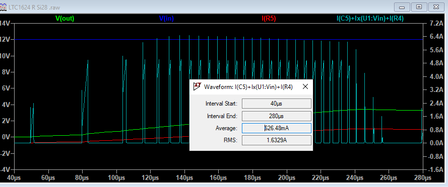


Fig. 1.11K: Current In Conductor between pin V1 IN and capacitor C5 1000p Over Time Period 40us - 280us


4.       The RMS value of the current is 1.6329A.

5.        The results over 1ms period of 907.73mA are tabulated in table 1.11C below:


Table 1.11C: Input Current Pin V1 of IN Over 1ms Period


LTspice Capacitor C5


1.      The current in the LTspice circuit in capacitor C5 1000p over 1ms period is shown 


          in the purple trace in the figure below:


Fig. 1.11L: Current in LTspice Capacitor C5

2.      The current in capacitor C5 1000p over 1ms period is 3.404mA

3.      Capacitor C5 1000p in LTspice is C2 1000pF in KiCad Eeschema.


Conductor LTspice Capacitor C5 1000p and pin Sense-  of U1 LTC1624 and R4 .033


1.    The current in the LTspice circuit in the lower conductor between C5 1000p and 

        pin Sense- of U1 LTC1624 and R4 .033 is shown by the light blue trace in 

        figure 1.11M  below:


Fig. 1.11M: conductor between LTspice Circuit C5 1000p and pin Sense- of U1 LTC1624 and R4 .033

2.      As can be seen, it is described as I(R4)+Ix(U2D) by the LTspice software and is 
  
         written in light blue at the top of the graph in the figure above. 

3.       It is the current in R4 .033 and Drain current U of U2 Si4128DY. 

4.       It is in total 3.43mA. 

5.       In KiCad Eeschema it is the current in the lower top horizontal conductor between 

          pin 1 ISENSE of U1 LTC1624CSB and Drain current pins 5, 6, 7, 8 of U2

           SI4128DY_T1-GE3.


LTspice Pin Vin of U1 LTC1624


1.     In the LTspice circuit the current flows into pin Vin of U1 LTC1624 is shown in the 


        light blue trace in figure 1.11N below:


Fig. 1.11N: Current flowing Into Pin Vin of U1 LTC1624


2.      This current is 6.4948mA.

3.      In the KiCad Eeschema circuit, it is the current that flows into 

         pin 8 VIN of U1 LTC1624CSB.


4. A summary of the currents calculated above by LTspice are shown in table 1.11D below:


Table 1.11D


Current In LTspice Circuit Capacitor C2 100p


1.      In the LTspice circuit current in C2 100p capacitor is shown in the light blue trace in 

        the figure below:


Fig. 1.11O: Current In Capacitor C2 100p in LTspice Circuit

2.        In the LTspice circuit the current in capacitor C2 100p is 354.8nA. 

3.        In KiCad Eeschema it is capacitor C1 100pF.


Current In Capacitor C4 0.1u In LTspice Circuit


1.      In the LTspice circuit the current in capacitor C4 0.1u is shown in the light blue trace 

        in figure 1.11P below:


Fig. 1.11P: Current in Capacitor C4 0.1uF in LTspice Circuit


2.      The current is 54.69mA. 

3.       In KiCad Eeschema it is referred to as C4 0.1uF.


The Current In Diode D1 MBRS340 In The LTspice Circuit 


1.     The current in the LTspice circuit in diode D1 MBRS340 is shown in the light blue 

        trace in figure 1.11Q below:


Fig. 1.11Q: Current In Diode D1 MBRS230 In LTspice Circuit

2.       Current in the diode D1 MBRS340 is 1.7209A. 

3.        The Kicad Eeschema diode is referred to as D1 MBRS340.


Current In The Conductor Between Pin Tg of U1 LTC1624 And Pin G of U2 Si4128DY


1.      In the LTspice circuit the current in the conductor between pin Tg of U1 LTC1624 

        and pin G of U2 Si4128DY is shown by the light blue trace in figure 1.11R below:


Fig. 1.11R: Current Between Pin Tg of U1 LTC1624 and Pin G of U2 Si4128Dy


3.      In the LTspice circuit the current between pin Tg of U1 LTC1624 and pin G of U2 

         Si4128DY is 14.396mA. 

4.      In the Kicad Eeschema circuit the conductor is between pin 6 TG of U1 LTC1624CSB

         and pin 4 Gate of U2 SI4128DY-T1-G3.

5.      Summary of calculations done above are summarized as follows in table 1.11E below:


Table 1.11E


Current In The Conductor In LTspice Circuit Between Pin FB of U1 LTC1624 

And R2  35.7K And R1 20K 


1.       The current in the conductor in LTspice Circuit between pin FB of U1 LTC1624 and 

          R2 35.7K and R1 20K is shown in the light blue trace in figure 1.11S below:


Fig. 1.11S: Current In The Conductor  Between Pin FB of U1 LTC1624 and R2 35.7K and R1 20K


2.      The current in the conductor in the LTspice circuit between pin FB of U1 LTC1624 

         and R2 35.7K and R1 20K is 374.34nA. 

3.     The KiCad Eeschema description of this conductor is the conductor between 

         pin 3 SET of U1 LTC1624CSB and R2 35.7k and R3 20k.


Current In Capacitor C1 200u In The LTspice Circuit 


1.      The current in capacitor C1 200u in the LTspice circuit is shown in the light blue 

         trace in figure 1.11R below:


Fig. 1.11R: Current In Capacitor C1 200u In LTspice Circuit


2.     The current in capacitor C1 200u in LTspice circuit is 1.627A. 

3.      The KiCad Eeschema description of this capacitor is C5 200uF. 

4.      The calculations done above are tabulated in table 1.11F:


Table 1.11F


KiCad Eeschema Circuit With All The Relevant Currents 


The KiCad Eeschema circuit with all the relevant currents is shown in figure 1.11S below:


Fig. 1.11S: KiCad Eeaschema Circuit With Currents Indicated


Conclusion

From the above we can classify the currents into two groups:

1.       Currents that range from 354.8nA to 63.165mA and are below 100mA; and


2.        Currents that range from 671.75mA to 1.9488A  and are below 2A.


Previous: Tutorial 1.10: Assign Footprints To Switching Regulator and MOSFET Transistor.


Monday, 30 September 2019

Tutorial 1.10: Assign Footprints to Switching Regulator and MOSFET Transistor


The footprint for Switching Regulator Controller LTC1624CS8

Check Footprint Assigned to Switching Regulator


1.        The next symbol 14 which is   U1 -    LTC1624CS8.

2.        KiCad has allocated the footprint Package_SO:SOIC-8_3.9x4.9mm_P1.27mm.

3.        Right-click on symbol 14 which is  U1 – LTC1824CS8 and select View Footprint.

4.        You should see the footprint as shown in figure 1.10A below:


Footprint Allocated By KiCad to U1 Switching Regulator Controller
Fig. 1.10A: Footprint Allocated By KiCad to U1 Switching Regulator Controller.


5.       From the SOIC-8_3.9x4.9mm_P1.27mm footprint name and measurements made 

          by the Vernier caliper or Measure distance between two points tool we 

          can conclude:

           5.1      SOIC - it is a Small Outline Integrated Circuit which is a surface- 

                        mounted integrated circuit (IC).

           5.2      8 – it has 8 pins.

           5.3      3.9x4.9mm – the IC has a horizontal body width of 3.9mm and a 

                        vertical length of 4.9mm.

          5.4      P1.27mm – the pin spacing is 1.27mm. 

          5.5     The total measured vertical length of all the pads included =  4.40mm.
             
          5.6     The total measured internal horizontal width between the pads = 3.00mm.

          5.7     Total measured external width between the pads included = 6.92mm.

6.      If we measure the pads with the Vernier caliper or Measure distance between two 

         points tool the horizontal width of a pad is 2.00mm and the vertical height of a pad

          is 0.6mm.

7.      If we get the datasheet from Linear Technology on the LTC1624 we see the LTC1624

          is a High-Efficiency SO-8 N-Channel Switching Regulator Controller as shown 

          in figure 1.10B below:


LTC1624: High-Efficiency Switching Regulator Controller Datasheet
Fig. 1.10B: LTC1624: High-Efficiency Switching Regulator Controller Datasheet


8.     From the datasheet, the package description of the LTC1624 is as shown in 

        figure 1.10C below.


Package of LTC1624 Switching Regulator Controller
Fig. 1.10C: Package of LTC1624 Switching Regulator Controller.


8.     It is described as having an S8 Package 8-Lead Plastic Small Outline.

9.      In the datasheet, the body width is given as between (3.810 – 3.988)mm, compared

         with 3.9mm given in KiCad footprint.

10.    In the datasheet, the body length is given between (4.801 – 5.004)mm, compared 

         with 4.9mm given in KiCad footprint.

11.    In the datasheet, the pin spacing is given as 1.270mm typically, compared with 

         1.27mm given in the KiCad footprint.

12.    In the datasheet, the pin width is given as between (0.355 – 0.483)mm, compared 

         in the KiCad footprint, this is measured in that the pad has a width or vertical 

         height of 0.6mm. This, of course, acceptable as the pads must be wider than the 

         pin width. 

13.    In the datasheet, the pin length is given as between (0.406 – 1.270)mm, compared 

         in the KiCad footprint, this is measured in that the pad has a horizontal width 

         or length of 2.00mm. This, of course, acceptable as the pads must be longer 

         than the pin length.  

14.     In the datasheet, if three-pin spacings as given in the datasheet is taken as 

          1.27mm x 3 = 3.81mm plus the width of a pin as given as 0.483mm 

          which is 3.81mm + 0.483mm= 4.293mm. 

         That can be compared with the total vertical length of all the pads included =  

         4.40mm measured in the KiCad footprint. 

15.     In the datasheet, the total internal width between the pads is estimated as  

          a worst case shortest distance is 5.791mm - (2x1.270mm =2.54mm) = 3.251mm. 

          This should be compared with the KiCad footprint where the total internal width 

          between the pads is measured at 3.00mm.

16.     In the datasheet, the total external width between the pads is given as (5.791 - 

          6.197)mm when compared with the KiCad footprint is measured at 6.92mm.

17.     It, therefore, seems this footprint as allocated by KiCad is fine.


Download Footprint From Ultra Librarian And Check Footprint


You can watch this video on YouTube cab licking on Download Footprint From Ultra 


Footprint for the MOSFET N-CH 30V 10.9A 8-SOIC SI4128DY-T1-GE3

Create a KiCad Footprint Library File


1.     Go to the Digi-Key website for the SI4128-T1-GE3 by clicking on

        Digi-Key Si4128DY

2.     You will see the description of the MOSFET N-CH 30V 10.9A 8-SOIC 

        SI4128DY-T1-GE3 as shown in figure 1.10D below:


Information On the SI4128DY-T1-GE3 as It Appears on the Digikey Website.
Fig. 1.10D: Information On the SI4128DY-T1-GE3 as It Appears on the Digikey Website.


3.     As you can see, they suggest we download the footprint or EDA/CAD Models from 

        Ultra Librarian.

4.      First, open a library file where you store your KiCad footprints.

5.      In KiCad the footprint library files have a .pretty extension.

6.       I made a library file, which I called “KICADFootprints” where I store all my 

          KiCad footprints. 

7.      I left out the .pretty extension.

8.      I suggest you create your file with a short path like right on your C drive.

9.       I suggest you call it something like: “MyKiCadFootprints.pretty”.

10.     The KiCad footprints themselves have a .kicad_mod extension.

11.     The KiCad footprints (files with a .kicad_mod file extension) themselves are 

           grouped in the particular library (file with .pretty extension). 

Create a Path to Your KiCad Library File


1.     You have to tell KiCad where your new footprints, the footprints that you add are.

2.     To do this you must create a path to your new library file.

3.     The library file is the file with the .pretty extension.

4.    You add the path in the Footprint Libraries window.

5.     To get there open the Assign Footprints window.

6.      Now click on Preferences then Manage Footprint Libraries… .

7.      Open the Footprint Libraries window.

8.      I generally put my footprints in the Global Libraries.

9.      Click on the envelope icon at the bottom or Add existing library to table.

10.     Navigate to where your KiCad footprint library file is. 

11.     In my case, it is C:/KICADFootprints.

12.     After you have finished it should be as in figure 1.10E below:


KICADFootprints Library Added
Fig. 1.10E: KICADFootprints Library Added


Download Footprint for MOSFET N-CH 30V 10.9A 8-SOIC SI4128DY-T1-GE3


1.       Go to Ultra Librarian by clicking on Ultra Librarian

2.       Type in "SI4128" in the search box.

3.        Download the footprint for SI4128DY-T1-GE3.

4.        Extract the SI4128DY-T1-GE3.kicad_mod footprint to your KiCad 

            footprint library file. 

5.        As mentioned in my case it is KICADFootprints.

5.        In the Assign Footprints window choose your KiCad footprint library.

6.        Right-click on the SI4128-Ti_GE3 Ultra Librarian file and select View Footprint.

7.       The footprint shown below in figure 1.10F should appear:


Fig. 1.10F: Ultra Librarian Si4128-T1-GE3 Footprint

8.       You can download the Vishay Siliconix datasheet by clicking on datasheet

9.      The package information of the SI4128 is shown in figure 1.10G below:


Package Information of SI4128
Fig. 1.10G: Package Information of SI4128


10.      From the package information, we can see the following applies:

           10.1      It is SOIC a Small Outline Integrated Circuit which is a surface- 

                        mounted integrated circuit (IC).

           10.2      It has 8 pins.

           10.3      The IC has a horizontal body width E of 3.8 - 4.00 mm. The 

                        measured width in the Footprint Editor is 4.0mm.

           10.4      The IC has a vertical length D of 4.9 - 5.0 mm. The 

                        measured vertical length in the Footprint Editor is 4.96mm.

           10.5      The IC has a horizontal body width of 3.9mm and a 

                        vertical length of 4.9mm and can, therefore, be written as 3.9x4.9mm

           10.6      The pin spacing is given as e = 1.27mm. The measured pin spacing in

                         the Footprint Editor is 1.27mm.

          10.7       The pin spacing is 1.27mm 

11.     According to KiCad, the footprint naming conventions are shown in figure 1.10H

         should be used for naming SMD IC package footprints.
Kicad naming conventions for surface mount integrated circuits.
Fig. 1,10H: Kicad naming conventions for surface mount integrated circuits.

12.      Taking into account the dimensions we already have and the KiCad 

           naming convention the footprint should be named as: 

           SOIC-8_3.9x4.9mm_P1.27mm


Vishay Recommended Minimum Pads


1.       According to the Vishay Siliconix datasheet the following minimum 
       
          pads are recommended for the Si4128DY N-Channel 30-V (D-S) MOSFET and 

          are shown in figure 1.10I below: 


Footprint for Si4128 as Recommended by Vishay
Fig. 1.10I: Footprint for Si4128 as Recommended by Vishay.


2.       Comparing the Vishay datasheet recommendation with the Vernier caliper tool or 

          Measure distance between two points measurements

         we can measure as follows:

          2.1       Horizontal  pad width (as in KiCad footprint)

                       2.1.1      Vishay datasheet recommendation is 1.194mm.

                       2.1.2      Pad in footprint measured = 1.66mm.

                       2.1.3     This is acceptable as it means the pad in the footprint is a bit wider.


          2.2       Vertical  pad height (as in KiCad footprint) 

                      2.2.1    Vishay datasheet recommendation of 0.559mm.

                      2.2.2     Vertical pad length in footprint measured = 0.55mm.

                      2.2.3     This is acceptable as they are virtually the same.


           2.3       External overall horizontal width of all pads included (as in KiCad footprint)

                       2.3.1    Vishay datasheet recommendation of 6.248mm. 

                       2.3.2    External width measured in footprint = 6.93mm. 
                     
                       2.3.3    This is acceptable as the footprint is a bit wider than the
      
                                   recommendation. Remember the footprint has longer horizontal

                                   width.

            2.4      The internal overall horizontal width between the pads 

                      (as in KiCad footprint)

                       2.4.1     Vishay datasheet recommendation of 3.861mm.

                       2.4.2     Measured in the footprint itself = 3.60mm.  

                       2.4.3    This is acceptable as it simply means that the pads in the footprint

                                     are slightly closer to each other when measured horizontally.
                       

            2.5       External overall vertical  length of all pads included (as in KiCad footprint)

                       2.5.1      Vishay datasheet recommendation of 4.369mm.

                       2.5.2      Measured overall external length = 4.37mm.

                       2.5.3      This is acceptable as it is virtually the same.


3.      We can, therefore, say the footprint we downloaded from Ultra Librarian is fine.


Assign Footprint to MOSFET Transistor


1.      Open the Assign Footprints window.

2.      In the middle window Symbol: Footprint Assignments click on 

        15   U2 -    SI4128DY-T1-GE3: 

3.     In the Filtered Footprints window on the right, double left click on 

        SI4128-T1-GE3.

4.    The final footprint assignments should look as shown in figure 1.10H shown below.


Fig. 1.10H: Final Footprint Assignments


5.      Click Apply, Save Schematic & Continue.

6.      Click OK.